Project Structure
| V4L2 FPGA |
|---|
 |
| Introduction |
| Getting the Code |
| Examples |
| GStreamer Pipelines |
| Supported Platforms |
| Contact Us |
Project Structure
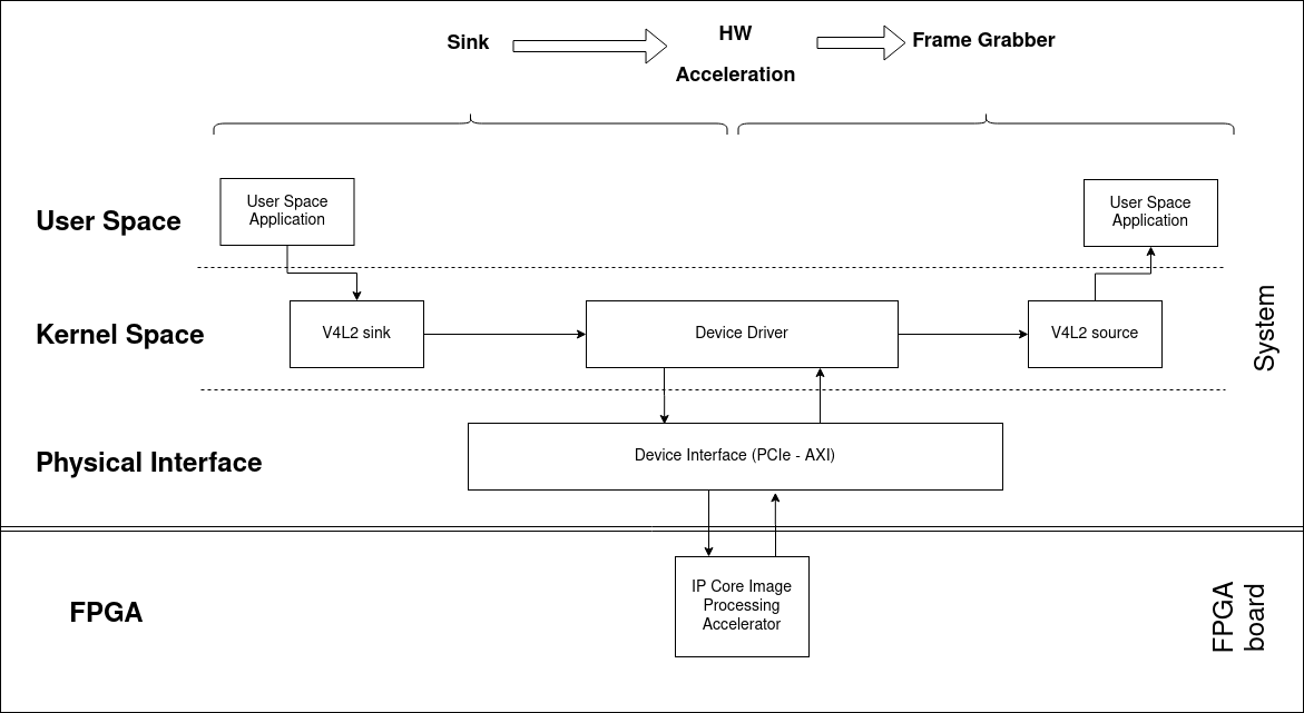
This project consists of three subsystems that allow for the acceleration of algorithms on custom hardware as shown in the following image:

Frame Sink: allows sending video frames from a user application to an FPGA device connected through either PCI-e or AXI. From the architecture perspective, a design could only have a Frame Sink and a hardware accelerator for controlling a display or a series of devices, which interact with the incoming video stream.
HW accelerator: this subsystem allows for the processing of frames by complex algorithms. Algorithms implemented in hardware are less power-intensive, faster, and allow for massive parallelism. An example of an HW accelerator is a demosaicing accelerator, which involves three convolutions running simultaneously at 8 pixels per clock each.
Frame Grabber: allows capturing frames from a FPGA device. A possible design can only have this subsystem, making it possible to connect a camera to the FPGA directly and perform the deserializing, decoding, and demosaicing without adding any overhead to the system processor, which will receive the frames ready for their consumption.
Each of the mentioned subsystems can work independently. Thus, you can have only one out of the three for your architecture and boost your application up.
With this project, it is possible to implement:
- Image processing applications: Bayer demosaicing, object detection and tracking, image filtering, and so on.
- Artificial Neural Networks: Since the transmission of data is in matrices, it is possible to implement interesting Artificial Intelligence applications.
- Massive signal processing applications: You can transmit and process multiple signals at the same time fitting them into matrices.
The applications can go beyond thanks to the FPGA configuration flexibility.
We also offer a HLS templated library with IP Cores for Image Signal Processing. You can visit FPGA Image Signal Processor project for more information.
FPGA
A Field Programmable Gate Array (FPGA) is an integrated circuit that can be configured after manufacturing. The FPGA allows implementing heavy computational algorithms described as hardware and offering massive parallelism, which leads to multi-pipeline architectures and vectorial computing.
One of the key strengths of FPGA is its capability of implementing software algorithms on hardware, which can be run at one computation per clock or even more, depending on the optimization techniques employed for parallelizing during the hardware description. In the field of Image Processing, custom image processing applications can be described as hardware on FPGA. It allows accelerating algorithms to the limits and achieving better performance in terms of GLOPS/Watt, resulting in high-performance computation with a lower consumption than GPUs.
Another main advantage of the FPGA is the possibility of reconfiguring it on-demand, making it possible to change the accelerators when they are required.
PCIe
PCI Express is a high-speed communication standard. PCI-e slots can contain multiple lanes allowing for further speed-up by transmitting information in each slot by parallel. PCI-e is the common interface for devices with high bandwidth requirements such as GPUs, Wi-Fi cards, Solid-State disks, and now FPGAs.
| Version | Bandwidth (per lane) | Bandwidth (per lane in a 16x slot) |
|---|---|---|
| PCIe 1.0 | 2 Gbit/s | 32 Gbit/s |
| PCIe 2.0 | 4 Gbit/s | 64 Gbit/s |
| PCIe 3.0 | 7.877 Gbit/s | 126.032 Gbit/s |
| PCIe 4.0 | 15.752 Gbit/s | 252.032 Gbit/s |
PCI-e compatible cards also come in a Mini Card factor which has a more flexible physical specification to connect to the PCIe bus, one example of these cards is the PicoEVB board, which allows connecting an FPGA to laptops or embedded systems.
AXI
The Advanced eXtensible Interface (AXI), part of the ARM Advanced Microcontroller Bus Architecture (AMBA), is a parallel high-performance, synchronous, high-frequency, multi-master, multi-slave communication interface, mainly designed for on-chip communication. It allows ARM-based processors to communicate to peripherals at high-speed, allowing those to communicate directly to the main memory (DDR) arbitrated by a DMA device. You may be interested in using this protocol if:
- Your device is a FPGA-based SoC.
- Your device is a custom ASIC with an ARM Microprocessor.
The speed may vary due to several factors: system bus clock, DDR speed, and peripheral frequency.
V4L2
Video4Linux is a collection of drivers and a common API for supporting real-time video capture on Linux systems.
The V4L2 provides a video capture interface to get video data from a tuner or camera device, a video output interface that can provide video images outside of the device.
The API also implements code that enables applications to discover a given device's capabilities and to configure the device to operate in the desired manner. These include cropping, frame rates, video compression, image parameters, video formats, etc.


